
This document is aimed at providing 13.56 MHz RFID systems designers with a practical cookbook on how to optimize RFID systems and antennas. A thorough analysis of the most important RFID system parameters is presented. The emphasis is placed on physical concepts, rather than on lengthy theoretical calculations.
Antenna? You said Antenna?
In the wireless world, antennas are used to transmit radio frequency energy from location A to location Bin the most efficient manner. That is they do radiate the power that is fed to them. If we were dealing with UHF RFID systems, this hypothesis would be true. However, at 13.56MHz, the picture is quite different. The wavelength in free space at 13.56 MHz is

A standard ground plane antenna has a length of one quarter of the wavelength which is 5.53 meters. It has a radiation resistance close to 50 ohms. In the world of 13.56 MHz RFID systems, we are unlikely to come close to such dimensions. And even if we do, the amount of radiated power will remain quite small. Let us consider an example. Say that we have a loop antenna and that its area is one square meter. The radiation resistance is given by:
In our case, this yields RR=130 milliohms and we probably have used 4 meters of wire to construct the loop, assuming a square shape… So, if we do not radiate energy, how do we transfer it to the tag we intend to communicate with?

The answer is magnetic coupling. Some people refer to RFID base stations as “couplers”. This terminology is certainly quite appropriate in our case. We have indeed to consider the RFID system, antenna plus tag, as a loosely coupled transformer, with the base station antenna acting as the primary of this transformer. This concept is of paramount importance for the system designer. One must always remember it. The tag AND the base station “antenna” constitute THE system, and cannot be studied separately. The other point to remember is that if we feed five Watts to a loop RFID “antenna”, these five Watts, being NOT radiated, will have to be dissipated somewhere…
Coupled circuits
In the preceding paragraph, we surreptitiously introduced another important, to say the least, concept. We said that we had a loosely coupled transformer. The complete theory of coupled circuits is beyond the scope of this document. It involves quite lengthy calculations, but we can somewhat alleviate this burden thanks to the use of a circuit simulator like SPICE. Now, we must define the characters, and assign a role to each of them.
The first character is our base station antenna. In order to maximize the communication range with the tag, we must create the strongest possible magnetic field, so that the tag will be able to pick up enough power in order to energize itself. Since the magnetic field from the loop is proportional to the current flowing through the conductor that actually constitutes the loop, we have to maximize this current.
The second character is the tag. The tag wants to be able to collect in as much energy as possible from the ambient magnetic field generated by the base station loop antenna. We must maximize this energy gathering capacity.
These goals can be achieved in various ways. However, the next paragraphs will show that the art of RFID system design requires a careful understanding of the pitfalls and conflicts that will inevitably arise. Our characters are not team players. More often than not they are unfair to each other.
The Q conflict:
From our base station antenna point of view, there is only one way to have a strong current flowing trough the conductors: the loop has to be tuned and made resonant. The same holds true for the tag. And here comes the first problem. If we had no data to transmit back and forth, we could increase the Q factor of both devices up to the tolerances or the components used. This would be the best way on both sides to fulfil our characters requirements. However, if we design a system to be compliant with the ISO 15693 standard, we have a sub carrier at 423 KHz, possibly ON/OFF keyed if we use the single sub carrier modulation at a data rate of 27 kBits/sec. For the ISO 14443 standard, the sub carrier is at 847 kHz, and the data rate is 106 kBits/sec. A tuned circuit acts as a band pass filter. We must leave enough bandwidth for the sub carrier and its modulation side bands.
Minimum bandwidth requirements from the tag point of view:
Let us take a look at how the tag modulation sees the tag antenna. In most cases, a tag can be modeled as a parallel resonant circuit (first order approximation). The modulation spectrum can be approximated quite accurately. On the following graph, we have represented the tag frequency response for a Q value of 12 (deep green curve), along with the ISO15693 single sub carrier /ASK power spectrum for a pseudo random bit sequence. We can see that the tag modulation is attenuated by about 1 dB, which is acceptable.

However, if we take a tag with a Q factor of about 16 (red curve), we find that the modulation peaks are attenuated by 3dB. And this is a limit that should not be trespassed otherwise the communication range between the base station and the tag could be severely affected. In practice, the optimal Q value will be chosen between 9 and 16, depending on other system constraints that we are going to analyze later.

The calculation of the modulation power spectrum is more complicated in the FSK double sub carrier case. However, it yields essentially the same results, as can be seen on the following graph. For the ISO 1443 standard, the modulation power spectrum is similar to an ASK spectrum for part A and part B. The only difference is the sub carrier frequency which is higher. This will of course change the Q requirement for the tag, it will have to be lower. The tag optimum Q will range from 4 to 9. We can now define a set of rules for the minimum bandwidth requirements, as seen from the tag point of view:
BW = FTOL + FSUB + DataRate ( for single sub carrier / ASK mode )
BW = FTOL + FSUB + DataRate( for double sub carrier FSK, or BPSK mode)
Where: BW is the minimum bandwidth, that is fc/2*Q, fc = 13.56 MHz.
FTOL is the frequency tolerance of the tuned circuit.
FSUB is the sub carrier frequency. And we must have

Minimum bandwidth requirements from the base station antenna point of view:
The base station antenna point of view is exactly the same as the tag antenna point of view. In fact, the base station antenna must have enough bandwidth to recover the tag modulation. The base station sends commands to the tag by direct modulation of the 13.56 MHz carrier. The protocol does not use a sub carrier for the base station to tag communications, and for both ISO standards, the data rates and modulation techniques used yield spectrums that have much smaller bandwidths than the tag. Therefore, for all practical purposes, we can say that the minimum system bandwidth requirements are set by the tag modulation spectrum. However, we must emphasize again that this assertion is only valid when the tag and the base station antenna are loosely coupled.
One should also consider these bandwidth requirements only as a good starting point, and always remember that only experimental results should say the final word. For instance, it might be possible that designing a base station antenna with a slightly higher Q than what theory suggests will increase the reading range, because the magnetic field strength improvement will outweigh the reduction in the tag backscatter signal strength.
How to calculate the coupling factor:
The nice thing is that the coupling factor depends only on geometrical parameters. The inductance values, the coils number of turns, are not involved. Let us consider the following oversimplified representation of a base station antenna coil and a tag antenna coil:

On the left, we have the base station antenna coil, with a diameter d1=2 x r1. On the right, we have the tag antenna coil, with a diameter d2=2 x r2, tilted along the axis by an angle . The coupling factor can be expressed as:

Of course, this equation is valid only for circular coils, but the design guidelines we are going to infer from it are valid whatever the shape. From the equation above, it is obvious that the coupling factor will be maximum when r1 = r2.
Getting out of the inferno:
In order to avoid a situation were the coupling factor would be too high, we can use different strategies:
We can design a system where the base station antenna is much larger than the tag coil. This is generallythe case for long range systems.
We can design a system where the base station antenna is much larger than the tag coil. This is generallythe case for long range systems.
For a short range system, where the sizes may be comparable, we must sacrifice the communicationrange to system reliability. This can be done by using a much lower Q for the tags. We can also deliberately mistune the tags.
The most critical situation will be for medium range systems, where antenna sizes are not sufficiently different to prevent coupling factor frequency spreading at short range. In that case, one is advised to maintain, by means of a physical obstacle, a minimum distance between the tag and the antenna in order to maintain the system in a functional state. Also, the output power stage driving the base station antenna MUST be resistant to mismatch. Even medium power stages can die quickly if they do not see the right load.
However, for short and medium range systems, an angel comes to our rescue and will mitigate the devil’s actions. All tags have a maximal power supply voltage. To protect the chip from an over voltage condition, the chip manufacturers usually place a pair of zener diodes that will start to conduct before the limit is reached in parallel with the coil inputs. When the diodes are placed in strong conduction, they effectively completely destroy the tag Q factor. This is very important because, in most cases, the coupling factor’s deleterious effects are sufficiently alleviated to maintain the system in a functional state.


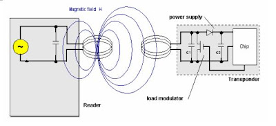
 The power P2 reflected from the transponder is radiated into free space. A small proportion of this (free space attenuation) is picked up by the reader's antenna. The reflected signal therefore travels into the antenna connection of the reader in the "backwards direction" and can be decoupled using a directional coupler and transferred to the receiver input of a reader. The "forward" signal of the transmitter, which is stronger by powers of ten, is to a large degree suppressed by the directional coupler.