
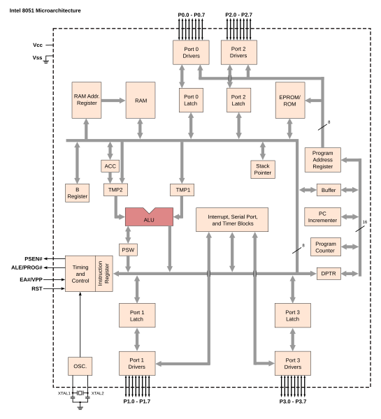
Introduction
.jpg)
The Intel 8051 is a Harvard architecture, single chip microcontroller (µC) which was developed by Intel in 1980 for use in embedded systems. Intel's original versions were popular in the 1980s and early 1990s, but has today largely been superseded by a vast range of faster and/or functionally enhanced 8051-compatible devices manufactured by more than 20 independent manufacturers including Atmel, Infineon Technologies (formerly Siemens AG), Maxim Integrated Products (via its Dallas Semiconductor subsidiary), NXP (formerly Philips Semiconductor), Nuvoton (formerly Winbond), ST Microelectronics, Silicon Laboratories (formerly Cygnal), Texas Instruments and Cypress Semiconductor. Intel's official designation for the 8051 family of µCs is MCS 51.
Intel's original 8051 family was developed using NMOS technology, but later versions, identified by a letter C in their name (e.g., 80C51) used CMOS technology and were less power-hungry than their NMOS predecessors. This made them more suitable for battery-powered devices.
Important features and applications
- It provides many functions (CPU, RAM, ROM, I/O, interrupt logic, timer, etc.) in a single package
- 8-bit ALU, Accumulator and 8-bit Registers; hence it is an 8-bit microcontroller
- 8-bit data bus - It can access 8 bits of data in one operation
- 16-bit address bus - It can access 216 memory locations - 64 KB (65536 locations) each of RAM and ROM
- On-chip RAM - 128 bytes (data memory)
- On-chip ROM - 4 kByte (program memory)
- Four byte bi-directional input/output port
- UART (serial port)
- Two 16-bit Counter/timers
- Two-level interrupt priority
- Power saving mode

A particularly useful feature of the 8051 core is the inclusion of a boolean processing engine which allows bit-level boolean logic operations to be carried out directly and efficiently on internal registers and RAM. This feature helped cement the 8051's popularity in industrial control applications. Another valued feature is that it has four separate register sets, which can be used to greatly reduce interrupt latency compared to the more common method of storing interrupt context on a stack.
The 8051 UARTs make it simple to use the chip as a serial communications interface. External pins can be configured to connect to internal shift registers in a variety of ways, and the internal timers can also be used, allowing serial communications in a number of modes, both synchronous and asynchronous. Some modes allow communications with no external components. A mode compatible with an RS-485 multi-point communications environment is achievable, but the 8051's real strength is fitting in with existing ad-hoc protocols (e.g., when controlling serial-controlled devices).
Once a UART, and a timer if necessary, have been configured, the programmer needs only to write a simple interrupt routine to refill the send shift register whenever the last bit is shifted out by the UART and/or empty the full receive shift register (copy the data somewhere else). The main program then performs serial reads and writes simply by reading and writing 8-bit data to stacks.
8051 based microcontrollers typically include one or two UARTs, two or three timers, 128 or 256 bytes of internal data RAM (16 bytes of which are bit-addressable), up to 128 bytes of I/O, 512 bytes to 64 kB of internal program memory, and sometimes a quantity of extended data RAM (ERAM) located in the external data space. The original 8051 core ran at 12 clock cycles per machine cycle, with most instructions executing in one or two machine cycles. With a 12 MHz clock frequency, the 8051 could thus execute 1 million one-cycle instructions per second or 500,000 two-cycle instructions per second. Enhanced 8051 cores are now commonly used which run at six, four, two, or even one clock per machine cycle, and have clock frequencies of up to 100 MHz, and are thus capable of an even greater number of instructions per second. All SILabs, some Dallas and a few Atmel devices have single cycle cores.
Common features included in modern 8051 based microcontrollers include built-in reset timers with brown-out detection, on-chip oscillators, self-programmable Flash ROM program memory, bootloader code in ROM, EEPROM non-volatile data storage, I²C, SPI, and USB host interfaces, CAN or LIN bus, PWM generators, analog comparators, A/D and D/A converters, RTCs, extra counters and timers, in-circuit debugging facilities, more interrupt sources, and extra power saving modes.
Types of Memory
The 8051 has three very general types of memory. To effectively program the 8051 it is necessary to have a basic understanding of these memory types.
The memory types are illustrated in the following graphic. They are: On-Chip Memory, External Code Memory, and External RAM.
On-Chip Memory refers to any memory (Code, RAM, or other) that physically exists on the microcontroller itself. On-chip memory can be of several types, but we'll get into that shortly.

External Code Memory is code (or program) memory that resides off-chip. This is often in the form of an external EPROM.
External RAM is RAM memory that resides off-chip. This is often in the form of standard static RAM or flash RAM.
Code Memory
Code memory is the memory that holds the actual 8051 program that is to be run. This memory is limited to 64K and comes in many shapes and sizes: Code memory may be found on-chip, either burned into the microcontroller as ROM or EPROM. Code may also be stored completely off-chip in an external ROM or, more commonly, an external EPROM. Flash RAM is also another popular method of storing a program. Various combinations of these memory types may also be used--that is to say, it is possible to have 4K of code memory on-chip and 64k of code memory off-chip in an EPROM.
When the program is stored on-chip the 64K maximum is often reduced to 4k, 8k, or 16k. This varies depending on the version of the chip that is being used. Each version offers specific capabilities and one of the distinguishing factors from chip to chip is how much ROM/EPROM space the chip has.
However, code memory is most commonly implemented as off-chip EPROM. This is especially true in low-cost development systems and in systems developed by students.
Programming Tip: Since code memory is restricted to 64K, 8051 programs are limited to 64K. Some assemblers and compilers offer ways to get around this limit when used with specially wired hardware. However, without such special compilers and hardware, programs are limited to 64K.
External RAM
As an obvious opposite of Internal RAM, the 8051 also supports what is called External RAM.
As the name suggests, External RAM is any random access memory which is found off-chip. Since the memory is off-chip it is not as flexible in terms of accessing, and is also slower. For example, to increment an Internal RAM location by 1 requires only 1 instruction and 1 instruction cycle. To increment a 1-byte value stored in External RAM requires 4 instructions and 7 instruction cycles. In this case, external memory is 7 times slower!
What External RAM loses in speed and flexibility it gains in quantity. While Internal RAM is limited to 128 bytes (256 bytes with an 8052), the 8051 supports External RAM up to 64K.
Programming Tip: The 8051 may only address 64k of RAM. To expand RAM beyond this limit requires programming and hardware tricks. You may have to do this "by hand" since many compilers and assemblers, while providing support for programs in excess of 64k, do not support more than 64k of RAM. This is rather strange since it has been my experience that programs can usually fit in 64k but often RAM is what is lacking. Thus if you need more than 64k of RAM, check to see if your compiler supports it-- but if it doesn't, be prepared to do it by hand.
On-Chip Memory
As mentioned at the beginning of this chapter, the 8051 includes a certain amount of on-chip memory. On-chip memory is really one of two types: Internal RAM and Special Function Register (SFR) memory. The layout of the 8051's internal memory is presented in the following memory map:

As is illustrated in this map, the 8051 has a bank of 128 bytes of Internal RAM. This Internal RAM is found on-chip on the 8051 so it is the fastest RAM available, and it is also the most flexible in terms of reading, writing, and modifying its contents. Internal RAM is volatile, so when the 8051 is reset this memory is cleared.
The 128 bytes of internal ram is subdivided as shown on the memory map. The first 8 bytes (00h - 07h) are "register bank 0". By manipulating certain SFRs, a program may choose to use register banks 1, 2, or 3. These alternative register banks are located in internal RAM in addresses 08h through 1Fh. We'll discuss "register banks" more in a later chapter. For now it is sufficient to know that they "live" and are part of internal RAM.
Bit Memory also lives and is part of internal RAM. We'll talk more about bit memory very shortly, but for now just keep in mind that bit memory actually resides in internal RAM, from addresses 20h through 2Fh.
The 80 bytes remaining of Internal RAM, from addresses 30h through 7Fh, may be used by user variables that need to be accessed frequently or at high-speed. This area is also utilized by the microcontroller as a storage area for the operating stack. This fact severely limits the 8051s stack since, as illustrated in the memory map, the area reserved for the stack is only 80 bytes--and usually it is less since this 80 bytes has to be shared between the stack and user variables.
Register Banks
The 8051 uses 8 "R" registers which are used in many of its instructions. These "R" registers are numbered from 0 through 7 (R0, R1, R2, R3, R4, R5, R6, and R7). These registers are generally used to assist in manipulating values and moving data from one memory location to another. For example, to add the value of R4 to the Accumulator, we would execute the following instruction:
ADD A,R4
Thus if the Accumulator (A) contained the value 6 and R4 contained the value 3, the Accumulator would contain the value 9 after this instruction was executed.
However, as the memory map shows, the "R" Register R4 is really part of Internal RAM. Specifically, R4 is address 04h. This can be see in the bright green section of the memory map. Thus the above instruction accomplishes the same thing as the following operation:
ADD A,04h
This instruction adds the value found in Internal RAM address 04h to the value of the Accumulator, leaving the result in the Accumulator. Since R4 is really Internal RAM 04h, the above instruction effectively accomplished the same thing.
But watch out! As the memory map shows, the 8051 has four distinct register banks. When the 8051 is first booted up, register bank 0 (addresses 00h through 07h) is used by default. However, your program may instruct the 8051 to use one of the alternate register banks; i.e., register banks 1, 2, or 3. In this case, R4 will no longer be the same as Internal RAM address 04h. For example, if your program instructs the 8051 to use register bank 3, "R" register R4 will now be synonomous with Internal RAM address 1Ch.
The concept of register banks adds a great level of flexibility to the 8051, especially when dealing with interrupts (we'll talk about interrupts later). However, always remember that the register banks really reside in the first 32 bytes of Internal RAM.
Programming Tip: If you only use the first register bank (i.e. bank 0), you may use Internal RAM locations 08h through 1Fh for your own use. But if you plan to use register banks 1, 2, or 3, be very careful about using addresses below 20h as you may end up overwriting the value of your "R" registers!
Bit Memory
The 8051, being a communications-oriented microcontroller, gives the user the ability to access a number of bit variables. These variables may be either 1 or 0.
There are 128 bit variables available to the user, numberd 00h through 7Fh. The user may make use of these variables with commands such as SETB and CLR. For example, to set bit number 24 (hex) to 1 you would execute the instruction:
SETB 24h
It is important to note that Bit Memory is really a part of Internal RAM. In fact, the 128 bit variables occupy the 16 bytes of Internal RAM from 20h through 2Fh. Thus, if you write the value FFh to Internal RAM address 20h youve effectively set bits 00h through 07h. That is to say that:
MOV 20h,#0FFh
is equivalent to:
SETB 00h
SETB 01h
SETB 02h
SETB 03h
SETB 04h
SETB 05h
SETB 06h
SETB 07h
As illustrated above, bit memory isnt really a new type of memory. Its really just a subset of Internal RAM. But since the 8051 provides special instructions to access these 16 bytes of memory on a bit by bit basis it is useful to think of it as a separate type of memory. However, always keep in mind that it is just a subset of Internal RAM--and that operations performed on Internal RAM can change the values of the bit variables.
Programming Tip: If your program does not use bit variables, you may use Internal RAM locations 20h through 2Fh for your own use. But if you plan to use bit variables, be very careful about using addresses from 20h through 2Fh as you may end up overwriting the value of your bits!
Bit variables 00h through 7Fh are for user-defined functions in their programs. However, bit variables 80h and above are actually used to access certain SFRs on a bit-by-bit basis. For example, if output lines P0.0 through P0.7 are all clear (0) and you want to turn on the P0.0 output line you may either execute:
MOV P0,#01h
or you may execute:
SETB 80h
Both these instructions accomplish the same thing. However, using the SETB command will turn on the P0.0 line without effecting the status of any of the other P0 output lines. The MOV command effectively turns off all the other output lines which, in some cases, may not be acceptable.
Programming Tip: By default, the 8051 initializes the Stack Pointer (SP) to 07h when the microcontroller is booted. This means that the stack will start at address 08h and expand upwards. If you will be using the alternate register banks (banks 1, 2 or 3) you must initialize the stack pointer to an address above the highest register bank you will be using, otherwise the stack will overwrite your alternate register banks. Similarly, if you will be using bit variables it is usually a good idea to initialize the stack pointer to some value greater than 2Fh to guarantee that your bit variables are protected from the stack.
Special Function Register (SFR) Memory
Special Function Registers (SFRs) are areas of memory that control specific functionality of the 8051 processor. For example, four SFRs permit access to the 8051s 32 input/output lines. Another SFR allows a program to read or write to the 8051s serial port. Other SFRs allow the user to set the serial baud rate, control and access timers, and configure the 8051s interrupt system.
When programming, SFRs have the illusion of being Internal Memory. For example, if you want to write the value "1" to Internal RAM location 50 hex you would execute the instruction:
MOV 50h,#01h
Similarly, if you want to write the value "1" to the 8051s serial port you would write this value to the SBUF SFR, which has an SFR address of 99 Hex. Thus, to write the value "1" to the serial port you would execute the instruction:
MOV 99h,#01h
As you can see, it appears that the SFR is part of Internal Memory. This is not the case. When using this method of memory access (its called direct address), any instruction that has an address of 00h through 7Fh refers to an Internal RAM memory address; any instruction with an address of 80h through FFh refers to an SFR control register.
Programming Tip: SFRs are used to control the way the 8051 functions. Each SFR has a specific purpose and format which will be discussed later. Not all addresses above 80h are assigned to SFRs. However, this area may NOT be used as additional RAM memory even if a given address has not been assigned to an SFR.
Special Function Registers
What Are SFRs?
The 8051 is a flexible microcontroller with a relatively large number of modes of operations. Your program may inspect and/or change the operating mode of the 8051 by manipulating the values of the 8051's Special Function Registers (SFRs).
SFRs are accessed as if they were normal Internal RAM. The only difference is that Internal RAM is from address 00h through 7Fh whereas SFR registers exist in the address range of 80h through FFh.
Each SFR has an address (80h through FFh) and a name. The following chart provides a graphical presentation of the 8051's SFRs, their names, and their address.
As you can see, although the address range of 80h through FFh offer 128 possible addresses, there are only 21 SFRs in a standard 8051. All other addresses in the SFR range (80h through FFh) are considered invalid. Writing to or reading from these registers may produce undefined values or behavior.
Programming Tip: It is recommended that you not read or write to SFR addresses that have not been assigned to an SFR. Doing so may provoke undefined behavior and may cause your program to be incompatible with other 8051-derivatives that use the given SFR for some other purpose.
SFR Types
As mentioned in the chart itself, the SFRs that have a blue background are SFRs related to the I/O ports. The 8051 has four I/O ports of 8 bits, for a total of 32 I/O lines. Whether a given I/O line is high or low and the value read from the line are controlled by the SFRs in green.
The SFRs with yellow backgrouns are SFRs which in some way control the operation or the configuration of some aspect of the 8051. For example, TCON controls the timers, SCON controls the serial port.
The remaining SFRs, with green backgrounds, are "other SFRs." These SFRs can be thought of as auxillary SFRs in the sense that they don't directly configure the 8051 but obviously the 8051 cannot operate without them. For example, once the serial port has been configured using SCON, the program may read or write to the serial port using the SBUF register.
Programming Tip: The SFRs whose names appear in red in the chart above are SFRs that may be accessed via bit operations (i.e., using the SETB and CLR instructions). The other SFRs cannot be accessed using bit operations. As you can see, all SFRs that whose addresses are divisible by 8 can be accessed with bit operations.
SFR Descriptions
This section will endeavor to quickly overview each of the standard SFRs found in the above SFR chart map. It is not the intention of this section to fully explain the functionality of each SFR--this information will be covered in separate chapters of the tutorial. This section is to just give you a general idea of what each SFR does.
P0 (Port 0, Address 80h, Bit-Addressable): This is input/output port 0. Each bit of this SFR corresponds to one of the pins on the microcontroller. For example, bit 0 of port 0 is pin P0.0, bit 7 is pin P0.7. Writing a value of 1 to a bit of this SFR will send a high level on the corresponding I/O pin whereas a value of 0 will bring it to a low level.
Programming Tip: While the 8051 has four I/O port (P0, P1, P2, and P3), if your hardware uses external RAM or external code memory (i.e., your program is stored in an external ROM or EPROM chip or if you are using external RAM chips) you may not use P0 or P2. This is because the 8051 uses ports P0 and P2 to address the external memory. Thus if you are using external RAM or code memory you may only use ports P1 and P3 for your own use.
SP (Stack Pointer, Address 81h): This is the stack pointer of the microcontroller. This SFR indicates where the next value to be taken from the stack will be read from in Internal RAM. If you push a value onto the stack, the value will be written to the address of SP + 1. That is to say, if SP holds the value 07h, a PUSH instruction will push the value onto the stack at address 08h. This SFR is modified by all instructions which modify the stack, such as PUSH, POP, LCALL, RET, RETI, and whenever interrupts are provoked by the microcontroller.
Programming Tip: The SP SFR, on startup, is initialized to 07h. This means the stack will start at 08h and start expanding upward in internal RAM. Since alternate register banks 1, 2, and 3 as well as the user bit variables occupy internal RAM from addresses 08h through 2Fh, it is necessary to initialize SP in your program to some other value if you will be using the alternate register banks and/or bit memory. It's not a bad idea to initialize SP to 2Fh as the first instruction of every one of your programs unless you are 100% sure you will not be using the register banks and bit variables.
DPL/DPH (Data Pointer Low/High, Addresses 82h/83h): The SFRs DPL and DPH work together to represent a 16-bit value called the Data Pointer. The data pointer is used in operations regarding external RAM and some instructions involving code memory. Since it is an unsigned two-byte integer value, it can represent values from 0000h to FFFFh (0 through 65,535 decimal).
Programming Tip: DPTR is really DPH and DPL taken together as a 16-bit value. In reality, you almost always have to deal with DPTR one byte at a time. For example, to push DPTR onto the stack you must first push DPL and then DPH. You can't simply plush DPTR onto the stack. Additionally, there is an instruction to "increment DPTR." When you execute this instruction, the two bytes are operated upon as a 16-bit value. However, there is no instruction that decrements DPTR. If you wish to decrement the value of DPTR, you must write your own code to do so.
PCON (Power Control, Addresses 87h): The Power Control SFR is used to control the 8051's power control modes. Certain operation modes of the 8051 allow the 8051 to go into a type of "sleep" mode which requires much less power. These modes of operation are controlled through PCON. Additionally, one of the bits in PCON is used to double the effective baud rate of the 8051's serial port.
TCON (Timer Control, Addresses 88h, Bit-Addressable): The Timer Control SFR is used to configure and modify the way in which the 8051's two timers operate. This SFR controls whether each of the two timers is running or stopped and contains a flag to indicate that each timer has overflowed. Additionally, some non-timer related bits are located in the TCON SFR. These bits are used to configure the way in which the external interrupts are activated and also contain the external interrupt flags which are set when an external interrupt has occured.
TMOD (Timer Mode, Addresses 89h): The Timer Mode SFR is used to configure the mode of operation of each of the two timers. Using this SFR your program may configure each timer to be a 16-bit timer, an 8-bit autoreload timer, a 13-bit timer, or two separate timers. Additionally, you may configure the timers to only count when an external pin is activated or to count "events" that are indicated on an external pin.
TL0/TH0 (Timer 0 Low/High, Addresses 8Ah/8Ch): These two SFRs, taken together, represent timer 0. Their exact behavior depends on how the timer is configured in the TMOD SFR; however, these timers always count up. What is configurable is how and when they increment in value.
TL1/TH1 (Timer 1 Low/High, Addresses 8Bh/8Dh): These two SFRs, taken together, represent timer 1. Their exact behavior depends on how the timer is configured in the TMOD SFR; however, these timers always count up. What is configurable is how and when they increment in value.
P1 (Port 1, Address 90h, Bit-Addressable): This is input/output port 1. Each bit of this SFR corresponds to one of the pins on the microcontroller. For example, bit 0 of port 1 is pin P1.0, bit 7 is pin P1.7. Writing a value of 1 to a bit of this SFR will send a high level on the corresponding I/O pin whereas a value of 0 will bring it to a low level.
SCON (Serial Control, Addresses 98h, Bit-Addressable): The Serial Control SFR is used to configure the behavior of the 8051's on-board serial port. This SFR controls the baud rate of the serial port, whether the serial port is activated to receive data, and also contains flags that are set when a byte is successfully sent or received.
Programming Tip: To use the 8051's on-board serial port, it is generally necessary to initialize the following SFRs: SCON, TCON, and TMOD. This is because SCON controls the serial port. However, in most cases the program will wish to use one of the timers to establish the serial port's baud rate. In this case, it is necessary to configure timer 1 by initializing TCON and TMOD.
SBUF (Serial Control, Addresses 99h): The Serial Buffer SFR is used to send and receive data via the on-board serial port. Any value written to SBUF will be sent out the serial port's TXD pin. Likewise, any value which the 8051 receives via the serial port's RXD pin will be delivered to the user program via SBUF. In other words, SBUF serves as the output port when written to and as an input port when read from.
P2 (Port 2, Address A0h, Bit-Addressable): This is input/output port 2. Each bit of this SFR corresponds to one of the pins on the microcontroller. For example, bit 0 of port 2 is pin P2.0, bit 7 is pin P2.7. Writing a value of 1 to a bit of this SFR will send a high level on the corresponding I/O pin whereas a value of 0 will bring it to a low level.
Programming Tip: While the 8051 has four I/O port (P0, P1, P2, and P3), if your hardware uses external RAM or external code memory (i.e., your program is stored in an external ROM or EPROM chip or if you are using external RAM chips) you may not use P0 or P2. This is because the 8051 uses ports P0 and P2 to address the external memory. Thus if you are using external RAM or code memory you may only use ports P1 and P3 for your own use.
IE (Interrupt Enable, Addresses A8h): The Interrupt Enable SFR is used to enable and disable specific interrupts. The low 7 bits of the SFR are used to enable/disable the specific interrupts, where as the highest bit is used to enable or disable ALL interrupts. Thus, if the high bit of IE is 0 all interrupts are disabled regardless of whether an individual interrupt is enabled by setting a lower bit.
P3 (Port 3, Address B0h, Bit-Addressable): This is input/output port 3. Each bit of this SFR corresponds to one of the pins on the microcontroller. For example, bit 0 of port 3 is pin P3.0, bit 7 is pin P3.7. Writing a value of 1 to a bit of this SFR will send a high level on the corresponding I/O pin whereas a value of 0 will bring it to a low level.
IP (Interrupt Priority, Addresses B8h, Bit-Addressable): The Interrupt Priority SFR is used to specify the relative priority of each interrupt. On the 8051, an interrupt may either be of low (0) priority or high (1) priority. An interrupt may only interrupt interrupts of lower priority. For example, if we configure the 8051 so that all interrupts are of low priority except the serial interrupt, the serial interrupt will always be able to interrupt the system, even if another interrupt is currently executing. However, if a serial interrupt is executing no other interrupt will be able to interrupt the serial interrupt routine since the serial interrupt routine has the highest priority.
PSW (Program Status Word, Addresses D0h, Bit-Addressable): The Program Status Word is used to store a number of important bits that are set and cleared by 8051 instructions. The PSW SFR contains the carry flag, the auxiliary carry flag, the overflow flag, and the parity flag. Additionally, the PSW register contains the register bank select flags which are used to select which of the "R" register banks are currently selected.
Programming Tip: If you write an interrupt handler routine, it is a very good idea to always save the PSW SFR on the stack and restore it when your interrupt is complete. Many 8051 instructions modify the bits of PSW. If your interrupt routine does not guarantee that PSW is the same upon exit as it was upon entry, your program is bound to behave rather erradically and unpredictably--and it will be tricky to debug since the behavior will tend not to make any sense.
ACC (Accumulator, Addresses E0h, Bit-Addressable): The Accumulator is one of the most-used SFRs on the 8051 since it is involved in so many instructions. The Accumulator resides as an SFR at E0h, which means the instruction MOV A,#20h is really the same as MOV E0h,#20h. However, it is a good idea to use the first method since it only requires two bytes whereas the second option requires three bytes.
B (B Register, Addresses F0h, Bit-Addressable): The "B" register is used in two instructions: the multiply and divide operations. The B register is also commonly used by programmers as an auxiliary register to temporarily store values.
Other SFRs
The chart above is a summary of all the SFRs that exist in a standard 8051. All derivative microcontrollers of the 8051 must support these basic SFRs in order to maintain compatability with the underlying MSCS51 standard.
A common practice when semiconductor firms wish to develop a new 8051 derivative is to add additional SFRs to support new functions that exist in the new chip. For example, the Dallas Semiconductor DS80C320 is upwards compatible with the 8051. This means that any program that runs on a standard 8051 should run without modification on the DS80C320. This means that all the SFRs defined above also apply to the Dallas component.
However, since the DS80C320 provides many new features that the standard 8051 does not, there must be some way to control and configure these new features. This is accomplished by adding additional SFRs to those listed here. For example, since the DS80C320 supports two serial ports (as opposed to just one on the 8051), the SFRs SBUF2 and SCON2 have been added. In addition to all the SFRs listed above, the DS80C320 also recognizes these two new SFRs as valid and uses their values to determine the mode of operation of the secondary serial port. Obviously, these new SFRs have been assigned to SFR addresses that were unused in the original 8051. In this manner, new 8051 derivative chips may be developed which will run existing 8051 programs.
Programming Tip: If you write a program that utilizes new SFRs that are specific to a given derivative chip and not included in the above SFR list, your program will not run properly on a standard 8051 where that SFR does not exist. Thus, only use non-standard SFRs if you are sure that your program wil only have to run on that specific microcontroller. Likewise, if you write code that uses non-standard SFRs and subsequently share it with a third-party, be sure to let that party know that your code is using non-standard SFRs to save them the headache of realizing that due to strange behavior at run-time.
Basic Registers
The Accumulator
If youve worked with any other assembly languages you will be familiar with the concept of an Accumulator register.
The Accumulator, as its name suggests, is used as a general register to accumulate the results of a large number of instructions. It can hold an 8-bit (1-byte) value and is the most versatile register the 8051 has due to the shear number of instructions that make use of the accumulator. More than half of the 8051s 255 instructions manipulate or use the accumulator in some way.
For example, if you want to add the number 10 and 20, the resulting 30 will be stored in the Accumulator. Once you have a value in the Accumulator you may continue processing the value or you may store it in another register or in memory.
The "R" registers
The "R" registers are a set of eight registers that are named R0, R1, etc. up to and including R7.
These registers are used as auxillary registers in many operations. To continue with the above example, perhaps you are adding 10 and 20. The original number 10 may be stored in the Accumulator whereas the value 20 may be stored in, say, register R4. To process the addition you would execute the command:
ADD A,R4
After executing this instruction the Accumulator will contain the value 30.
You may think of the "R" registers as very important auxillary, or "helper", registers. The Accumulator alone would not be very useful if it were not for these "R" registers.
The "R" registers are also used to temporarily store values. For example, lets say you want to add the values in R1 and R2 together and then subtract the values of R3 and R4. One way to do this would be:
MOV A,R3 ;Move the value of R3 into the accumulator
ADD A,R4 ;Add the value of R4
MOV R5,A ;Store the resulting value temporarily in R5
MOV A,R1 ;Move the value of R1 into the accumulator
ADD A,R2 ;Add the value of R2
SUBB A,R5 ;Subtract the value of R5 (which now contains R3 + R4)
As you can see, we used R5 to temporarily hold the sum of R3 and R4. Of course, this isnt the most efficient way to calculate (R1+R2) - (R3 +R4) but it does illustrate the use of the "R" registers as a way to store values temporarily.
The "B" Register
The "B" register is very similar to the Accumulator in the sense that it may hold an 8-bit (1-byte) value.
The "B" register is only used by two 8051 instructions: MUL AB and DIV AB. Thus, if you want to quickly and easily multiply or divide A by another number, you may store the other number in "B" and make use of these two instructions.
Aside from the MUL and DIV instructions, the "B" register is often used as yet another temporary storage register much like a ninth "R" register.
The Data Pointer (DPTR)
The Data Pointer (DPTR) is the 8051s only user-accessable 16-bit (2-byte) register. The Accumulator, "R" registers, and "B" register are all 1-byte values.
DPTR, as the name suggests, is used to point to data. It is used by a number of commands which allow the 8051 to access external memory. When the 8051 accesses external memory it will access external memory at the address indicated by DPTR.
While DPTR is most often used to point to data in external memory, many programmers often take advantge of the fact that its the only true 16-bit register available. It is often used to store 2-byte values which have nothing to do with memory locations.
The Program Counter (PC)
The Program Counter (PC) is a 2-byte address which tells the 8051 where the next instruction to execute is found in memory. When the 8051 is initialized PC always starts at 0000h and is incremented each time an instruction is executed. It is important to note that PC isnt always incremented by one. Since some instructions require 2 or 3 bytes the PC will be incremented by 2 or 3 in these cases.
The Program Counter is special in that there is no way to directly modify its value. That is to say, you cant do something like PC=2430h. On the other hand, if you execute LJMP 2430h youve effectively accomplished the same thing.
The Stack Pointer (SP)
The Stack Pointer, like all registers except DPTR and PC, may hold an 8-bit (1-byte) value. The Stack Pointer is used to indicate where the next value to be removed from the stack should be taken from.
When you push a value onto the stack, the 8051 first increments the value of SP and then stores the value at the resulting memory location.
When you pop a value off the stack, the 8051 returns the value from the memory location indicated by SP, and then decrements the value of SP.
This order of operation is important. When the 8051 is initialized SP will be initialized to 07h. If you immediately push a value onto the stack, the value will be stored in Internal RAM address 08h. This makes sense taking into account what was mentioned two paragraphs above: First the 8051 will increment the value of SP (from 07h to 08h) and then will store the pushed value at that memory address (08h).
SP is modified directly by the 8051 by six instructions: PUSH, POP, ACALL, LCALL, RET, and RETI. It is also used intrinsically whenever an interrupt is triggered (more on interrupts later. Dont worry about them for now!)
Addressing Modes
An "addressing mode" refers to how you are addressing a given memory location. In summary, the addressing modes are as follows, with an example of each:
Immediate Addressing MOV A,#20h
Direct Addressing MOV A,30h
Indirect Addressing MOV A,@R0
External Direct MOVX A,@DPTR
Code Indirect MOVC A,@A+DPTR
Each of these addressing modes provides important flexibility.
Immediate Addressing
Immediate addressing is so-named because the value to be stored in memory immediately follows the operation code in memory. That is to say, the instruction itself dictates what value will be stored in memory.
For example, the instruction:
MOV A,#20h
This instruction uses Immediate Addressing because the Accumulator will be loaded with the value that immediately follows; in this case 20 (hexidecimal).
Immediate addressing is very fast since the value to be loaded is included in the instruction. However, since the value to be loaded is fixed at compile-time it is not very flexible.
Direct Addressing
Direct addressing is so-named because the value to be stored in memory is obtained by directly retrieving it from another memory location. For example:
MOV A,30h
This instruction will read the data out of Internal RAM address 30 (hexidecimal) and store it in the Accumulator.
Direct addressing is generally fast since, although the value to be loaded isnt included in the instruction, it is quickly accessable since it is stored in the 8051s Internal RAM. It is also much more flexible than Immediate Addressing since the value to be loaded is whatever is found at the given address--which may be variable.
Also, it is important to note that when using direct addressing any instruction which refers to an address between 00h and 7Fh is referring to Internal Memory. Any instruction which refers to an address between 80h and FFh is referring to the SFR control registers that control the 8051 microcontroller itself.
The obvious question that may arise is, "If direct addressing an address from 80h through FFh refers to SFRs, how can I access the upper 128 bytes of Internal RAM that are available on the 8052?" The answer is: You cant access them using direct addressing. As stated, if you directly refer to an address of 80h through FFh you will be referring to an SFR. However, you may access the 8052s upper 128 bytes of RAM by using the next addressing mode, "indirect addressing."
Indirect Addressing
Indirect addressing is a very powerful addressing mode which in many cases provides an exceptional level of flexibility. Indirect addressing is also the only way to access the extra 128 bytes of Internal RAM found on an 8052.
Indirect addressing appears as follows:
MOV A,@R0
This instruction causes the 8051 to analyze the value of the R0 register. The 8051 will then load the accumulator with the value from Internal RAM which is found at the address indicated by R0.
For example, lets say R0 holds the value 40h and Internal RAM address 40h holds the value 67h. When the above instruction is executed the 8051 will check the value of R0. Since R0 holds 40h the 8051 will get the value out of Internal RAM address 40h (which holds 67h) and store it in the Accumulator. Thus, the Accumulator ends up holding 67h.
Indirect addressing always refers to Internal RAM; it never refers to an SFR. Thus, in a prior example we mentioned that SFR 99h can be used to write a value to the serial port. Thus one may think that the following would be a valid solution to write the value 1 to the serial port:
MOV R0,#99h ;Load the address of the serial port
MOV @R0,#01h ;Send 01 to the serial port -- WRONG!!
This is not valid. Since indirect addressing always refers to Internal RAM these two instructions would write the value 01h to Internal RAM address 99h on an 8052. On an 8051 these two instructions would produce an undefined result since the 8051 only has 128 bytes of Internal RAM.
External Direct
External Memory is accessed using a suite of instructions which use what I call "External Direct" addressing. I call it this because it appears to be direct addressing, but it is used to access external memory rather than internal memory.
There are only two commands that use External Direct addressing mode:
MOVX A,@DPTR
MOVX @DPTR,A
As you can see, both commands utilize DPTR. In these instructions, DPTR must first be loaded with the address of external memory that you wish to read or write. Once DPTR holds the correct external memory address, the first command will move the contents of that external memory address into the Accumulator. The second command will do the opposite: it will allow you to write the value of the Accumulator to the external memory address pointed to by DPTR.
External Indirect
External memory can also be accessed using a form of indirect addressing which I call External Indirect addressing. This form of addressing is usually only used in relatively small projects that have a very small amount of external RAM. An example of this addressing mode is:
MOVX @R0,A
Once again, the value of R0 is first read and the value of the Accumulator is written to that address in External RAM. Since the value of @R0 can only be 00h through FFh the project would effectively be limited to 256 bytes of External RAM. There are relatively simple hardware/software tricks that can be implemented to access more than 256 bytes of memory using External Indirect addressing; however, it is usually easier to use External Direct addressing if your project has more than 256 bytes of External RAM.
Program Flow
When an 8051 is first initialized, it resets the PC to 0000h. The 8051 then begins to execute instructions sequentially in memory unless a program instruction causes the PC to be otherwise altered. There are various instructions that can modify the value of the PC; specifically, conditional branching instructions, direct jumps and calls, and "returns" from subroutines. Additionally, interrupts, when enabled, can cause the program flow to deviate from its otherwise sequential scheme.
Conditional Branching
The 8051 contains a suite of instructions which, as a group, are referred to as "conditional branching" instructions. These instructions cause program execution to follow a non-sequential path if a certain condition is true.
Take, for example, the JB instruction. This instruction means "Jump if Bit Set." An example of the JB instruction might be:
JB 45h,HELLO
NOP
HELLO: ....
In this case, the 8051 will analyze the contents of bit 45h. If the bit is set program execution will jump immediately to the label HELLO, skipping the NOP instruction. If the bit is not set the conditional branch fails and program execution continues, as usual, with the NOP instruction which follows.
Conditional branching is really the fundamental building block of program logic since all "decisions" are accomplished by using conditional branching. Conditional branching can be thought of as the "IF...THEN" structure in 8051 assembly language.
An important note worth mentioning about conditional branching is that the program may only branch to instructions located withim 128 bytes prior to or 127 bytes following the address which follows the conditional branch instruction. This means that in the above example the label HELLO must be within +/- 128 bytes of the memory address which contains the conditional branching instruction.
Direct Jumps
While conditional branching is extremely important, it is often necessary to make a direct branch to a given memory location without basing it on a given logical decision. This is equivalent to saying "Goto" in BASIC. In this case you want the program flow to continue at a given memory address without considering any conditions.
This is accomplished in the 8051 using "Direct Jump and Call" instructions. As illustrated in the last paragraph, this suite of instructions causes program flow to change unconditionally.
Consider the example:
LJMP NEW_ADDRESS
.
.
.
NEW_ADDRESS: ....
The LJMP instruction in this example means "Long Jump." When the 8051 executes this instruction the PC is loaded with the address of NEW_ADDRESS and program execution continues sequentially from there.
The obvious difference between the Direct Jump and Call instructions and the conditional branching is that with Direct Jumps and Calls program flow always changes. With conditional branching program flow only changes if a certain condition is true.
It is worth mentioning that, aside from LJMP, there are two other instructions which cause a direct jump to occur: the SJMP and AJMP commands. Functionally, these two commands perform the exact same function as the LJMP command--that is to say, they always cause program flow to continue at the address indicated by the command. However, SJMP and AJMP differ in the following ways:
The SJMP command, like the conditional branching instructions, can only jump to an address within +/- 128 bytes of the SJMP command.
The AJMP command can only jump to an address that is in the same 2k block of memory as the AJMP command. That is to say, if the AJMP command is at code memory location 650h, it can only do a jump to addresses 0000h through 07FFh (0 through 2047, decimal).
You may be asking yourself, "Why would I want to use the SJMP or AJMP command which have restrictions as to how far they can jump if they do the same thing as the LJMP command which can jump anywhere in memory?" The answer is simple: The LJMP command requires three bytes of code memory whereas both the SJMP and AJMP commands require only two. Thus, if you are developing an application that has memory restrictions you can often save quite a bit of memory using the 2-byte AJMP/SJMP instructions instead of the 3-byte instruction.
Recently, I wrote a program that required 2100 bytes of memory but I had a memory restriction of 2k (2048 bytes). I did a search/replace changing all LJMPs to AJMPs and the program shrunk downto 1950 bytes. Thus, without changing any logic whatsoever in my program I saved 150 bytes and was able to meet my 2048 byte memory restriction.
NOTE: Some quality assemblers will actually do the above conversion for you automatically. That is, they'll automatically change your LJMPs to SJMPs whenever possible. This is a nifty and very powerful capability that you may want to look for in an assembler if you plan to develop many projects that have relatively tight memory restrictions.
Direct Calls
Another operation that will be familiar to seasoned programmers is the LCALL instruction. This is similar to a "Gosub" command in Basic.
When the 8051 executes an LCALL instruction it immediately pushes the current Program Counter onto the stack and then continues executing code at the address indicated by the LCALL instruction.
Returns from Routines
Another structure that can cause program flow to change is the "Return from Subroutine" instruction, known as RET in 8051 Assembly Language.
The RET instruction, when executed, returns to the address following the instruction that called the given subroutine. More accurately, it returns to the address that is stored on the stack.
The RET command is direct in the sense that it always changes program flow without basing it on a condition, but is variable in the sense that where program flow continues can be different each time the RET instruction is executed depending on from where the subroutine was called originally.
Interrupts
An interrupt is a special feature which allows the 8051 to provide the illusion of "multi-tasking," although in reality the 8051 is only doing one thing at a time. The word "interrupt" can often be subsituted with the word "event."
An interrupt is triggered whenever a corresponding event occurs. When the event occurs, the 8051 temporarily puts "on hold" the normal execution of the program and executes a special section of code referred to as an interrupt handler. The interrupt handler performs whatever special functions are required to handle the event and then returns control to the 8051 at which point program execution continues as if it had never been interrupted.
The topic of interrupts is somewhat tricky and very important. For that reason, an entire chapter will be dedicated to the topic. For now, suffice it to say that Interrupts can cause program flow to change.
Timing
In order to understand--and better make use of--the 8051, it is necessary to understand some underlying information concerning timing.
The 8051 operates based on an external crystal. This is an electrical device which, when energy is applied, emits pulses at a fixed frequency. One can find crystals of virtually any frequency depending on the application requirements. When using an 8051, the most common crystal frequencies are 12 megahertz and 11.059 megahertz--with 11.059 being much more common. Why would anyone pick such an odd-ball frequency? Theres a real reason for it--it has to do with generating baud rates and well talk more about it in the Serial Communication chapter. For the remainder of this discussion well assume that were using an 11.059Mhz crystal.
Microcontrollers (and many other electrical systems) use crystals to syncrhronize operations. The 8051 uses the crystal for precisely that: to synchronize its operation. Effectively, the 8051 operates using what are called "machine cycles." A single machine cycle is the minimum amount of time in which a single 8051 instruction can be executed. although many instructions take multiple cycles.
A cycle is, in reality, 12 pulses of the crystal. That is to say, if an instruction takes one machine cycle to execute, it will take 12 pulses of the crystal to execute. Since we know the crystal is pulsing 11,059,000 times per second and that one machine cycle is 12 pulses, we can calculate how many instruction cycles the 8051 can execute per second:
11,059,000 / 12 = 921,583
This means that the 8051 can execute 921,583 single-cycle instructions per second. Since a large number of 8051 instructions are single-cycle instructions it is often considered that the 8051 can execute roughly 1 million instructions per second, although in reality it is less--and, depending on the instructions being used, an estimate of about 600,000 instructions per second is more realistic.
For example, if you are using exclusively 2-cycle instructions you would find that the 8051 would execute 460,791 instructions per second. The 8051 also has two really slow instructions that require a full 4 cycles to execute--if you were to execute nothing but those instructions youd find performance to be about 230,395 instructions per second.
It is again important to emphasize that not all instructions execute in the same amount of time. The fastest instructions require one machine cycle (12 crystal pulses), many others require two machine cycles (24 crystal pulses), and the two very slow math operations require four machine cycles (48 crystal pulses).
NOTE: Many 8051 derivative chips change instruction timing. For example, many optimized versions of the 8051 execute instructions in 4 oscillator cycles instead of 12; such a chip would be effectively 3 times faster than the 8051 when used with the same 11.059 Mhz crystal.
Since all the instructions require different amounts of time to execute a very obvious question comes to mind: How can one keep track of time in a time-critical application if we have no reference to time in the outside world?
Instruction Set
8051 INSTRUCTION SET HERE
Note:- Instruction set depends on manufacturer
Leading Manufactures
Data sheets
Basic Intel 8051 click here
some others
Leading Manufactures
Data sheets
Basic Intel 8051 click here
some others
| Manufacturer | Part Number | CODE | Int RAM | Notes: |
|---|---|---|---|---|
| Atmel | - Any - | - | - | Architecture Desc |
| Philips | - Any - | - | - | Architecture Desc |
| Atmel | - Any - | - | - | Memory Organization |
| Philips | - Any - | - | - | Instruction Set + Other Useful Info |
| Atmel | - Any - | - | - | Instruction Set |
| Atmel | - Any - | - | - | Hardware Desc |
| Philips | - Any - | - | - | Hardware Desc |
| Analog Devices | ADuC816 | 8k | 256 | 16 Bit A/D, 12 Bit D/A, Flash ROM, EEPROM, I2C |
| Atmel | 89C52 | 8k | 256 | Flash ROM |
| Atmel | 89C2051 | 2k | 128 | Flash ROM, 20 pins |
| Dallas | 80C320 | Ext Req'd | 256 | High Speed, 2 UART |
| Dallas | 87C520 | 16k | 256 + 1k | High Speed, 2 UART |
| Dallas | 87C550 | 16k | 256 + 1k | HS, 2 UART, 10-bit A/D, PWM, More Pins |
| Philips | 87C52 | 8k | 256 | OTP EPROM |
| Philips | 87C552 | 8k | 256 | 10-bit A/D, I2C, PWM |
| Cygnal | C8051F000 | 32k | 256 | 12-bit A/D + analog functions, high speed CPU |
No comments:
Post a Comment