In simpler times, FPGA power consumption was a simpler issue. In the traditional applications of high-capacity FPGAs, such as expensive network routers, telecommunications switching gear, and prototype boards for ASIC designs, all you needed to know was how much peak power the FPGA could consume and how to provide cooling for its operating appetites. Today, the world is different. “Previously, FPGAs were not a serious alternative for production,” says Rahul Shah, director of customer solutions at design-services vendor eInfochips. “But with shorter life spans for products and more emphasis on time to market, we are seeing customers want to go into production with FPGAs. So, more focus is now going onto the power consumed in the FPGA.”

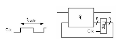
Facing tight enclosures with minimal cooling, tight budgets, and sometimes even battery power, designers must be able to get accurate power estimates on their FPGA designs early in the design cycle. They must be able to refine those estimates throughout the cycle so that they can apply aggressive power-management techniques (Figure 1). And they must be able to accurately measure the power of the resulting design. As it turns out, none of these requirements is trivial.
Early estimation
Ideally, design teams could begin to explore the power-consumption implications of their designs from the beginning, when they are formulating the design requirements and exploring algorithms. No widely used tools are available, however, for estimating power consumption from a set of design requirements or even from an algorithm. So, when the members of a design team have the most leverage over power consumption, they are flying nearly blind. Only experience with similar applications is there to guide them. “Our engagement with power issues begins at the specification stage,” says Raj Kothandaraman, lead FPGA designer at Wipro Technologies. The company built up an internal design method with an emphasis on power management. Through that method, design teams accumulate data—vital to early power estimates—on switching activity for various kinds of structures. Such history can give the design team some qualitative idea of the implications of the design requirements and even the power costs of algorithm decisions.
Shah describes a similar dependence on experience. “You define the power budget early, considering things you can know early, such as voltage levels, input-data characteristics, and the major functional blocks in the proposed system,” he says. “Often, we will look at static power first since it is less sensitive to detailed information that we won't have early in the design. Then, as we understand more about the design, we will begin estimating dynamic power, and, finally, we will begin to estimate the impact of power-saving strategies. There are no formal tools for this estimation process. So we have to rely on data-sheet information, spreadsheets, and our own experience with FPGAs.”
These early estimates are necessarily vague because much of the information necessary for an accurate estimate—detailed toggle-rate information, actual data flows, routing loads, and power-management features, for instance—doesn't yet exist. But it is still necessary to have a conservative estimate of the final system. Mike Morgan, principal design engineer at design shop North Pole Engineering, points out that the customer's decision to use an FPGA in the first place often results from a tight design schedule. That same pressure demands that the board design start concurrently with the FPGA design. And the board design, early on, needs estimated power. “In general, when I start a PCB [printed-circuit-board] design centered around a Xilinx device, I conservatively estimate power consumption and design or specify power supplies, distribution, and heat dissipation based on this [estimation],” he says.
Refining the estimates
As the design progresses from algorithms through definition of blocks and on to the beginnings of implementation, the design team gets more specific data about signals, toggle rates, and the structure of the blocks. At this point, still long before freezing the RTL (register-transfer-level) logic, design teams begin to use vendor-supplied power-estimation tools to improve the accuracy of their power estimates. “Tools from the FPGA vendor—typically, Excel spreadsheets—become important,” Kothandaraman says. These tools can absorb huge amounts of information about the design. For example, Ian Milton, a member of the technical staff at Altera, says that the company's Early Power Estimator allows designers to enter activity levels on registers, clock frequencies, enable-pin duty cycles, block-RAM configurations, read/write duty cycles, statistical characteristics of input signals, estimates of the number of logic elements in a block, and so on.
For the most part, vendors have designed these spreadsheets so that design teams can enter architectural information early, leave many of the inputs at default settings, and get a crude estimate of power. As the team learns more about the design, they can replace more of the defaults with design data, refining the power estimate. “We try to encourage people to use the default settings early on,” Milton says. The reason for relying on the defaults is that the vendors have built what amount to intelligent systems into those default settings, deriving defaults from actual measurements of large numbers of designs. For example, Altera's tool estimates how many of the nets in a design will have critical timing and how many will have timing slack and, employing that estimate, determines how many logic cells will be in high-performance mode and how many will be in low-leakage mode.
Even with the defaults, though, the design team still has to understand a great deal about the behavior—rather than the implementation—of the design to get the best estimate. “We look at input-data patterns,” says eInfochips' Shah. “From there, we look at clock-tree power. Then, we ask whether the inputs are going into a datapath or a control path and try to understand what that [placement] implies about the activity levels inside. There are no predefined calculations that will tell you these things. You have to rely on experience and methodology. You try to institutionalize the knowledge you gain from each new design by creating templates and processes. Unfortunately, the vendors have not defined a clear methodology for doing a power-aware design, so every design team around the world is doing this job in its own way.”
Wipro's Kothandaraman agrees that one of the most powerful weapons for using the early-estimate spreadsheets is experience. “For instance, we have estimates for I/O activity based on previous designs in the same application area,” he says. “That [information] is a great help in estimating the final power.”
The accuracy of these early estimates is an interesting issue. “These tools have really improved recently,” Kothandaraman says. “Years ago, there were lots of correlation problems with the tool results. But today, you can expect your early estimates to be within 20 or 30 percent of the final power consumption.”
Shah agrees. “Vendors are becoming more sensitive to power issues,” he says. “They are providing more accurate models and more Webinars on how to use the tools; this estimation process was not so accurate before.”
But Kothandaraman warns that the design process has a way of undermining its own power estimates. “As we go along, we tend to add more logic to the design,” he says. “That [tendency] kills our early power estimates.”
As the tools improve, the problems are getting more complex. A modern FPGA has multiple power rails, including core, auxiliary, I/O, and analog rails. All these rails are important in the analysis of parts, according to Jatinder Singh, an application engineer at Lattice Semiconductor. Each of these rails may be operating at a different voltage, and there may be two or more I/O voltages. Some devices may have separate core-power rails that you can shut down independently, and each of these power rails may respond to a different measure of activity. So the early-estimate spreadsheets must be explicit about separating activity in the logic fabric from I/O activity, monitoring SERDES (serializer/deserializer) activity as a separate issue, and so on. Further, the growing plethora of embedded functions in modern FPGAs adds complications. Estimates must encompass the configuration of and activity on DSP blocks and block RAMs, for instance.
Final estimates
As the design team creates RTL logic, the inputs to the spreadsheet estimators can become more precise. Once there is enough logic to perform simulation, however, a new category of vendor tool becomes available: the power analyzer.
These tools work in a fundamentally different way from spreadsheet estimators. “Once you have good RTL, you can synthesize and map the design,” says Altera's Milton. “Then, you can run a simulation and extract a value-change dump. This [step] will provide actual toggle rates on every node in a block.” A power analyzer reads this data, combines it with the mapping files that indicate the actual LUT (look-up-table) and routing-segment configuration at each node, and produces power calculations that, in principle, are as accurate as the vendor's device models. “The tools know things the customer couldn't know, such as the actual wire segments the mapping tool used to connect two logic elements,” Milton says. “And the tools understand the differences between FPGAs and ASICs. For example, in an ASIC, if you have an AND gate with one input low, there is no significant activity in the gate; the output is low. But, in an FPGA, the output buffer will stay low, but there is significant power-consuming activity within the LUT. Every change in the active input is causing, in effect, a read cycle in a little RAM.”
Power analyzers should be the last word in estimating the power consumption of an FPGA design. Accuracy is a two-edged sword, however. If you put in the wrong input data, you get precisely wrong results. One problem is trying to employ too precise a tool too early, according to eInfochips' Shah. “Don't update your power estimates with incomplete RTL,” he says. “That remaining few [percentage points] of the RTL may turn out to consume 30 percent of the power.”
Also, Shah warns that seemingly small changes to the RTL can make big changes in power consumption. “FPGA mapping is not as deterministic as ASIC layout,” he says. “Routing depends on the remaining resources in the device. If you are filling up the FPGA, you may find that LUTs that are connected to each other are nowhere near adjacent to each other.” Increased distance would increase power dissipation for each toggle of signals passing between the LUTs.
Wipro's Kothandaraman also counsels caution. “The power-analyzer tools do not always improve our understanding of the power consumption of our design,” he says. “Partly, this [drawback] is because we keep adding logic until late in the design. Also, the tools don't always do the most powerful job of processing the simulation dumps. And the value of the predictions depends on the value of the simulation scenarios you choose to run. But there are many operating modes in a modern FPGA design. It is a big challenge to generate vectors that will actually stimulate worst-case toggle rates.” On this last point, Kothandaraman says that Wipro is trying to establish a feedback loop within its design teams to capture experience in creating vectors for power estimation. But that work is still in progress.
The company knows from experience what worst-case traffic patterns should be for memory activity in networking equipment, for instance. In applications such as media processors or set-top boxes, however, identifying a worst-case video clip may take a major simulation effort all by itself. Kothandaraman adds that it is important to study not just logic-fabric activity, but also what's going on in the other parts of the FPGA. In both media and networking applications, memory blocks and SERDES may be more important to the power consumption than the logic fabric itself.
Another increasingly important variable comes from the fact that many system-in-FPGA designs now include microprocessor cores. This fact makes the power scenarios depend not only on the RTL logic, the mapping, and the vectors, but also on the firmware. Just as the hardware design team is freezing RTL logic and trying to pin down power data, the software team may be just getting working silicon and entering their period of highest rate of change for the firmware, with huge implications for power. The bottom line, according to Kothandaraman, is that you must make careful use of power-analysis tools. He warns that the early-estimation tools may end up giving you more accurate results than the analysis tools do.
Measuring the results
One big advantage of FPGAs is that, in the case of any uncertainly, you can always program up a part, drop it into a prototyping board, and see what it does. In the case of FPGA-power measurement, however, this problem is far from trivial. In part, measuring FPGA power is complicated because there are so many power rails and pins. In practice, the multiplicity of pins per rail means you have to measure voltage and current closer to the regulator, rather than closer to the chip, risking errors on high-current transients. It helps that most FPGA vendors provide access for current probes on their evaluation boards (Figure 2).

A more serious problem is that FPGA power-rail current tends to be dynamic. “As you move to finer geometries, the inrush current when you first apply power to an FPGA is often greater than the steady-state current,” says Lattice's Singh. “You must characterize SRAM-based FPGAs in three sections—inrush, initialization, and programming—in addition to steady-state current.”
Kothandaraman describes another problem. “On some devices, there is also a current pulse between the programming and operating modes,” he says.
North Pole's Morgan reports similar experience. “Once we have a prototype, power demands are one of many items we verify as part of the design-verification process,” he says. “We are most concerned with identifying the peak current demand [and] peak inrush and reporting the observed peak and average operating quiescent currents to ensure that our power supplies and dc/dc converters are operating optimally, traces and power vias are appropriately sized, junction temperatures do not exceed data-sheet specifications, and so on.” As Morgan points out, the dynamics on the power pins create their own measurement problems. Sudden bursts of activity in a highly parallel structure within the core or sudden bursts of memory traffic may produce narrow current spikes. These spikes may not contribute much to rms (root/mean/square) power, but they can fry metal on advanced-geometry FPGAs. The spikes also cause IR drops, which the decoupling-capacitor network needs to handle.
The problem is not getting any simpler. Vendors are making available more sophisticated power-management techniques, including clock gating, reduced-voltage operation, and some degree of power gating. According to one source, National Semiconductor is working with some FPGA designs to apply dynamic voltage-frequency scaling to the core-logic fabric of an FPGA, claiming that it is possible to achieve a 30 to 40 percent reduction in power in this way. Each of these techniques makes the problem of estimating—and measuring—power that much harder. Shah says that eInfochips often manipulates the configuration of FPGAs in the prototype, attempting to isolate a functional block and get an accurate power measurement on it. “This is an interesting problem,” he says. “Measuring power is a bit challenging on the board.”
Estimating and measuring FPGA power is a difficult problem. Design teams need early worst-case estimates and accurate data throughout the design to make decisions on power-management strategies. When they are done, they also need to know what they've accomplished. We can expect vendor tools to improve, but it may be deep experience in an application and with an FPGA architecture that ends up making the most difference.